TC55V400AFT-70 - [ TC55V400AFT-70 (A3) ]


Digital IC Shop
TC55V400AFT-70 - [ TC55V400AFT-70 (A3) ]
$16.07
262,144-WORD BY 16-BIT FULL CMOS STATIC RAM
DESCRIPTION
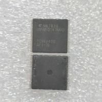
The TC55V400AFT is a 4,194,304-bit static random access memory (SRAM) organized as 262,144 words by 16
bits. Fabricated using Toshiba's CMOS Silicon gate process technology, this device operates from a single 2.3 to 3.6
V power supply. Advanced circuit technology provides both high speed and low power at an operating current of 3
mA/MHz and a minimum cycle time of 55 ns. It is automatically placed in low-power mode at 0.5 A standby
current (at VDD 3 V, Ta 25°C, maximum) when chip enable (CE1 ) is asserted high or (CE2) is asserted low.
There are three control inputs. CE1 and CE2 are used to select the device and for data retention control, and
output enable ( OE ) provides fast memory access. Data byte control pin ( LB , UB ) provides lower and upper byte
access. This device is well suited to various microprocessor system applications where high speed, low power and
battery backup are required. And, with a guaranteed operating extreme temperature range of 40° to 85°C, the
TC55V400AFT can be used in environments exhibiting extreme temperature conditions. The TC55V400AFT is
available in normal and reverse pinout plastic 48-pin thin-small-outline package (TSOP).
FEATURES
Low-power dissipation
Operating: 10.8 mW/MHz (typical)
Single power supply voltage of 2.3 to 3.6 V
Power down features usingCE1 and CE2
Data retention supply voltage of 1.5 to 3.6 V
Direct TTL compatibility for all inputs and outputs
Wide operating temperature range of 40° to 85°C
Buy Now : https://www.digitalicshop.com/product_info.php?products_id=&language=
262,144-WORD BY 16-BIT FULL CMOS STATIC RAM
DESCRIPTION
The TC55V400AFT is a 4,194,304-bit static random access memory (SRAM) organized as 262,144 words by 16
bits. Fabricated using Toshiba's CMOS Silicon gate process technology, this device operates from a single 2.3 to 3.6
V power supply. Advanced circuit technology provides both high speed and low power at an operating current of 3
mA/MHz and a minimum cycle time of 55 ns. It is automatically placed in low-power mode at 0.5 A standby
current (at VDD 3 V, Ta 25°C, maximum) when chip enable (CE1 ) is asserted high or (CE2) is asserted low.
There are three control inputs. CE1 and CE2 are used to select the device and for data retention control, and
output enable ( OE ) provides fast memory access. Data byte control pin ( LB , UB ) provides lower and upper byte
access. This device is well suited to various microprocessor system applications where high speed, low power and
battery backup are required. And, with a guaranteed operating extreme temperature range of 40° to 85°C, the
TC55V400AFT can be used in environments exhibiting extreme temperature conditions. The TC55V400AFT is
available in normal and reverse pinout plastic 48-pin thin-small-outline package (TSOP).
FEATURES
Low-power dissipation
Operating: 10.8 mW/MHz (typical)
Single power supply voltage of 2.3 to 3.6 V
Power down features usingCE1 and CE2
Data retention supply voltage of 1.5 to 3.6 V
Direct TTL compatibility for all inputs and outputs
Wide operating temperature range of 40° to 85°C
![]() The product data sheet can be downloaded by clicking here
The product data sheet can be downloaded by clicking here