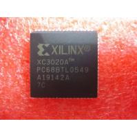
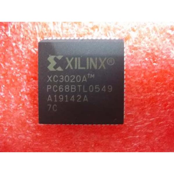
XC3020A-7PC68C - [ XC3020A-7PC68C (A1) ]

Digital IC Shop
XC3020A-7PC68C - [ XC3020A-7PC68C (A1) ]
5,000Ft
XC3000-Series Field Programmable Gate Arrays (FPGAs)
provide a group of high-performance, high-density, digital
integrated circuits. Their regular, extendable, flexible,
user-programmable array architecture is composed of a
configuration program store plus three types of configurable elements: a perimeter of I/O Blocks (IOBs), a core
array of Configurable Logic Bocks (CLBs) and resources
for interconnection. The general structure of an FPGA is
shown in Figure 2. The development system provides
schematic capture and auto place-and-route for design
entry. Logic and timing simulation, and in-circuit emulation
are available as design verification alternatives. The design
editor is used for interactive design optimization, and to
compile the data pattern that represents the configuration
program.
The FPGA user logic functions and interconnections are
determined by the configuration program data stored in
internal static memory cells. The program can be loaded in
any of several modes to accommodate various system
requirements. The program data resides externally in an
EEPROM, EPROM or ROM on the application circuit
board, or on a floppy disk or hard disk. On-chip initialization
logic provides for optional automatic loading of program
data at power-up. The companion XC17XX Serial Configuration PROMs provide a very simple serial configuration
program storage in a one-time programmable package.
The XC3000 Field Programmable Gate Array families provide a variety of logic capacities, package styles, temperature ranges and speed grades.
Buy Now : https://www.digitalicshop.com/product_info.php?products_id=&language=en
XC3000-Series Field Programmable Gate Arrays (FPGAs)
provide a group of high-performance, high-density, digital
integrated circuits. Their regular, extendable, flexible,
user-programmable array architecture is composed of a
configuration program store plus three types of configurable elements: a perimeter of I/O Blocks (IOBs), a core
array of Configurable Logic Bocks (CLBs) and resources
for interconnection. The general structure of an FPGA is
shown in Figure 2. The development system provides
schematic capture and auto place-and-route for design
entry. Logic and timing simulation, and in-circuit emulation
are available as design verification alternatives. The design
editor is used for interactive design optimization, and to
compile the data pattern that represents the configuration
program.
The FPGA user logic functions and interconnections are
determined by the configuration program data stored in
internal static memory cells. The program can be loaded in
any of several modes to accommodate various system
requirements. The program data resides externally in an
EEPROM, EPROM or ROM on the application circuit
board, or on a floppy disk or hard disk. On-chip initialization
logic provides for optional automatic loading of program
data at power-up. The companion XC17XX Serial Configuration PROMs provide a very simple serial configuration
program storage in a one-time programmable package.
The XC3000 Field Programmable Gate Array families provide a variety of logic capacities, package styles, temperature ranges and speed grades.
![]() The product data sheet can be downloaded by clicking here
The product data sheet can be downloaded by clicking here


